
This is a summary of an article originally published on SemiWiki by Kalar Rajendiran on May 4, 2026.
Advanced nodes, heterogeneous integration, and AI-driven design are making semiconductor development more complex every year. The article argues that infrastructure is an underappreciated constraint, and that the traditional model of building and running ECAD IT in-house is getting harder to sustain.
The Growing Infrastructure Burden
Modern chip workflows depend on distributed compute, EDA toolchains from multiple vendors, GPU-heavy AI/ML workloads, and strict security and compliance requirements. Teams often have to stitch together cloud and on-prem systems, license servers, and orchestration tools while keeping uptime high. Cloud providers and EDA vendors each supply part of the answer, but there is no widely available, production-ready, vendor-agnostic environment for semiconductor engineering, so teams fill the gap themselves.
The Limits of the Build-It-Yourself Model
Closing that gap means CAD engineering teams, DevOps and cloud specialists, and custom scripts. That offers flexibility, but it brings heavy upkeep, and misconfigurations, workflow failures, and wasted resources are common. The effort also does little to differentiate the product being designed.
A Shift Toward Engineering Infrastructure Platforms
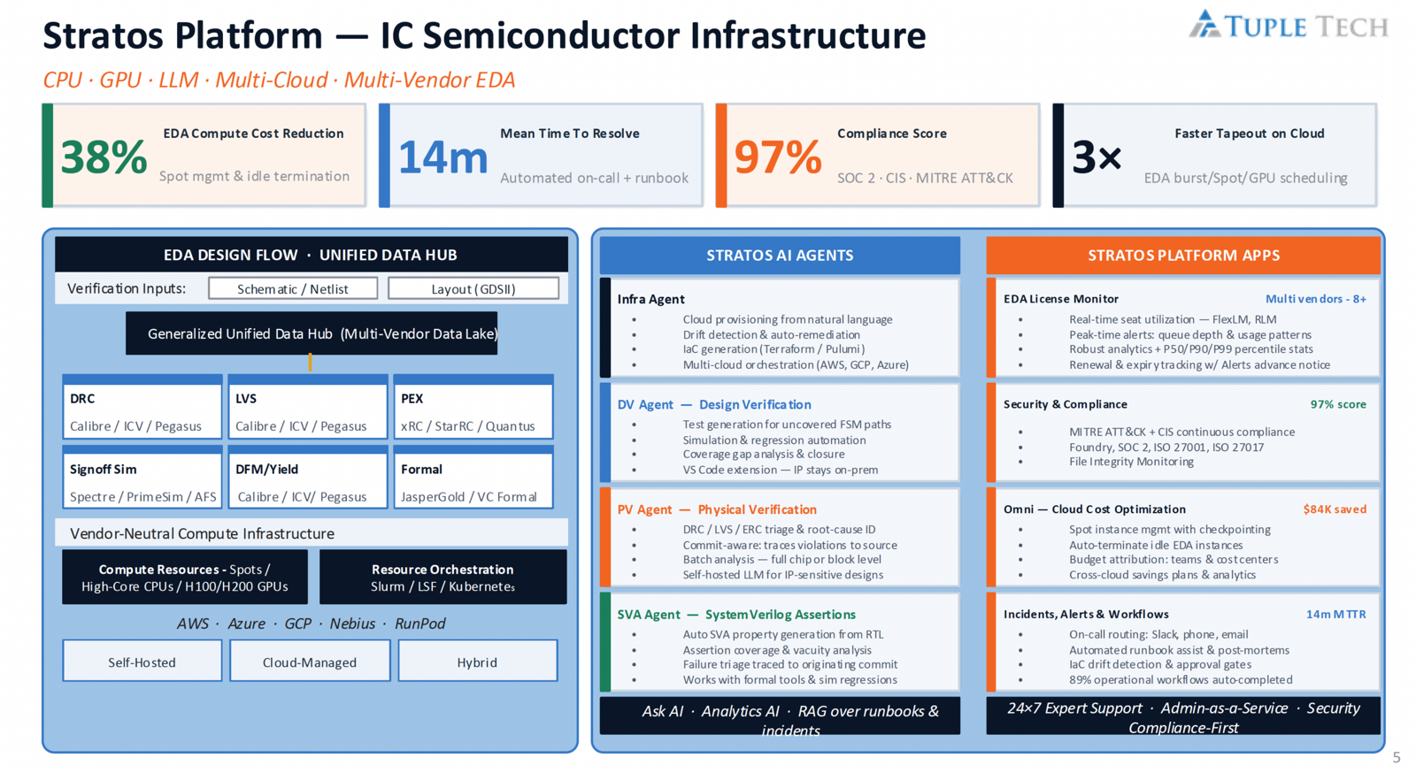
The alternative described is a platform with pre-integrated environments, vendor-neutral tool support, automated orchestration, and built-in observability and security. It hides infrastructure complexity without giving up flexibility. Tuple Tech's Stratos is presented as an example, with environments provisioned in minutes rather than weeks across self-hosted, cloud, and hybrid setups, including AI and HPC workloads.
What Changes with a Platform Approach
Stratos is built on Infrastructure-as-Code principles. The article lists fast provisioning, support for multiple EDA vendors without lock-in, integration of AI and HPC workloads into existing flows, and continuous monitoring with automated remediation. Engineers can focus on design, and CAD teams no longer have to manage licenses by hand, debug workflows, or coordinate across scattered environments.
Quantifiable Impact
The article cites the following figures, attributed to Tuple Tech and a customer case study:
- Up to 70% reduction in infrastructure development time
- Provisioning in minutes instead of weeks
- An average 38% reduction in GPU and compute costs through multi-cloud optimization
- A 43% reduction in cloud computing costs for Pegasus sign-off workloads, from a customer case study
It also points to better license utilization through real-time analytics, less downtime from proactive incident management, and faster disaster recovery through IaC-based rebuilds.
Key Differentiators
- Vendor neutrality: combine tools from multiple vendors without fragmenting workflows.
- Multi-cloud optimization: run workloads wherever compute is most efficient.
- Operational intelligence: monitoring and escalation that detect and resolve failures automatically.
- Built-in security: continuous compliance and threat detection.
- Domain-specific support: engineers who understand semiconductor workflows.
Why This Matters Now
As designs grow more data- and compute-intensive, infrastructure becomes a key enabler of engineering productivity. Companies that rely on fragmented, manually managed environments risk slower time-to-market, higher costs, and lower engineering efficiency. The article concludes that moving from fragmented systems to unified engineering platforms is the next frontier for the industry.